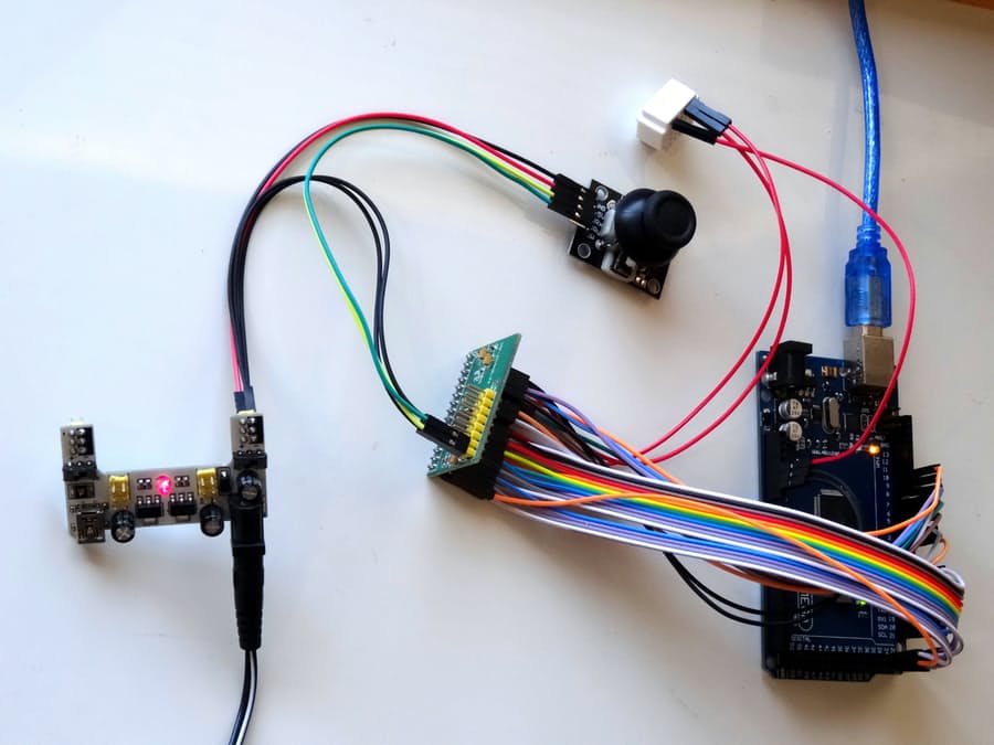
AD7606 DATA Acquisition Module 200Ksps 16Bits ADC 8CH Synchronization
http://www.icstation.com/ad7606-data-acquisition-module-200ksps-16bits-synchronization-p-7367.html

Description
1. using high-precision 16-bit ADC chip AD7606
2. 8 analog inputs. 1M ohm impedance. [No negative supply, there is no
front-end analog amplifier can be connected directly to the sensor
output]
3. the input range of plus or minus 5V, plus or minus 10V. By IO control.
4. Resolution 16.
5. the maximum sampling frequency sampling rate of 200ksps. Supports
eight sampling settings file (which can effectively reduce the jitter)
6. built-in benchmark
7. a single 5V power supply
8. SPI Interface, or 16-bit bus interface. Interface IO level can be 5V or 3.3V.
We AD7606 module factory default is 16bit parallel interface.
If SPI interface mode, you need to modify R1 R2 resistor configuration.
(8080 8bit)Parallel Mode Jumper: R1 floating (not stickers), R2 10K resistor paste
SPI interface mode jumper: R1 floating (not stickers), R2 10K resistor paste
AD7606 configuration is very simple, it has no internal registers.
Range and over-sampling parameters are controlled via an external IO.
Pulse frequency sampling rate provided by the microcontroller or DSP control.
AD7606 must use a single 5V supply.
Level communication interface between the AD7606 and SCM controlled
by VIO pin. That VIO power supply must be connected to the
microcontroller can be 3.3V can also be 5V.
Module Pin Description
OS2 OS1 OS2: a combination of state selection oversampling mode.
000 means no oversampling, the maximum sampling rate of 200ksps.
001 represents two times oversampling, which is the hardware inside collected two samples averaging
010 represents four times oversampling, which is the hardware inside collect four samples averaged
011 represents eight times oversampling, which is the hardware inside collected eight samples averaged
100 represents 16 times oversampling, which is the hardware inside collected 16 samples averaged
101 represents 32 times oversampling, which is an internal hardware averaging collected 32 samples
110 represents 64 times oversampling, which is the hardware inside collected 64 samples averaged
Oversampling ratio is higher, the longer the ADC conversion time, the lower the maximum sampling frequency can be obtained.
CVA, CVB: AD conversion start control signal channel 1-4 decision CVA, CVB decided 5-8 channels.
Two signals can stagger a short time, in general, can be CVA, CVB parallel together.
RAGE: Select the range of 0 means plus or minus 5V, 1 indicates negative 10V.
RD: Read signal
RST: Reset signal
Busy: Busy Signal
CS: chip-select signal
FRST: first a channel samples indicating signal
VIO: communication interface level
DB0 - DB15: Data Bus
[16 parallel mode wiring diagram --- AD7606 also supports 8-bit bus mode, see the AD7606 data sheet
MCU side AD7606 module
GND <----- ground
+5 V <----- 5V power supply
RAGE <----- can also be connected to the GPIO connected fixed level
OS2 <----- can also be connected to the GPIO connected fixed level
OS1 <----- can also be connected to the GPIO connected fixed level
OS0 <----- can also be connected to the GPIO connected fixed level
CVA <----- access the GPIO (output) is used to start AD conversion [Recommended pick pin with PWM output capability]
CVB <--- |
RD <----- 8080 bus read signal NOE
RST <----- GPIO output hardware reset AD606
Busy -----> GPIO input AD606 being converted instructions. [Recommended connection with external pin interrupt capability]
CS <----- 8080 bus chip select NCS
VIO <----- microcontroller power supply
DB0-DB15 -----> 8080 data bus (16)
FRST may take
[SPI interface mode wiring diagram
MCU side AD7606 module
GND <----- ground
+5 V <----- 5V power supply
RAGE <----- any output GPIO, can be accessed by a fixed level
OS2 <----- any output GPIO, can be accessed by a fixed level
OS1 <----- any output GPIO, can be accessed by a fixed level
OS0 <----- any output GPIO, can be accessed by a fixed level
CVA <----- access the GPIO (output) is used to start AD conversion [Recommended pick pin with PWM output capability]
CVB <--- |
RD / SCLK <----- SPI bus clock SCK
RST <----- any output GPIO, for hardware reset AD606
Busy -----> GPIO input, AD606 being converted instructions. [Recommended connection with external pin interrupt capability]
CS <----- SPI bus chip select SCS
VIO <----- microcontroller power supply
DB7 (DOUTA) -----> SPI bus data lines MISO
DB14 - DB15 may pick
FRST may take
Reviewed by ICStation's Partner Boian Mitovhttps://www.hackster.io/mitov/connect-ad7606-8-channel-16-bit-adc-in-16-bit-parallel-mode-4a6cfc


没有评论:
发表评论